What Makes a Thin-Film Electrode Good
Why NeuroNexus silicon probes and thin-film grids: the four determinants of electrode quality, how each is controlled, the support behind them, and the record.
20 min read
Updated October 27, 2026

NeuroNexus · neuronexus.com · Resources
A thin-film electrode is good when every site is where the design says it is, reads the impedance its area predicts, stays insulated for the life of the experiment, reaches the headstage through a package that does not fail first, and is backed by the people who made it. NeuroNexus has designed, fabricated, packaged, and supported silicon probes and thin-film polymer grids for more than 20 years; this paper sets out the determinants of electrode quality, how NeuroNexus controls each, and the published record that results.
Research use only. NeuroNexus products are for non-clinical research use and must not be used in human or veterinary medical procedures.
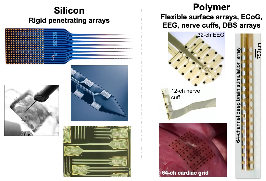
Figure 1. The two NeuroNexus thin-film electrode platforms. (Left) Silicon: rigid penetrating arrays, from a 256-site Buzsáki-layout die to the shank tip and the wafer. (Right) Polymer: flexible surface arrays for EEG, nerve, heart, and deep brain stimulation.
Not all thin-film electrodes are created equal. Two probes can share a specification, 32 sites at 100 µm pitch, 177 µm² iridium, a 5 mm shank, and behave differently in the same preparation, because a specification describes a design and says nothing about how faithfully it was made, what it was made of, how it was packaged, or who stands behind it. Electrode quality has four determinants: the design, the fabrication process, the materials, and the package assembly. Each leaves a signature a researcher can measure before a probe goes in, and each is where a thin-film electrode is either engineered or merely drawn. Two further things decide whether an electrode serves a study: the technical support behind it, and the record of what others have done with it. The sections below take them in order, with the published evidence for each.
Why are two electrodes with the same specification not the same electrode?#
A specification is a statement about a design; a probe is a design that has been through a process. The thin-film process deposits and patterns conductive and dielectric (insulating) layers on a wafer, and every step has a tolerance: a site can be smaller than drawn, a trace narrower or thinner, a dielectric layer can have a pinhole, a via can be incomplete. None of these appears in a specification, and each changes what the probe records.
The specification also says nothing about what happens after the wafer. An electrode array becomes a usable probe when it has a package: the bonds from the pads to the interconnect, the insulation over those bonds, the body that mounts it, and the connector that mates it to a headstage. A high-quality array on a low-quality package is a low-quality probe.
So the question "is this a good electrode?" has four parts, and they are not interchangeable. The design decides whether the probe can answer the experimental question. The fabrication process decides whether the probe is the design. The materials decide how the probe behaves at the interface and how long it lasts. The package decides whether any of it reaches the amplifier, and for how long.
What does the design decide?#
The design decides what the probe can see. Probe geometry, the shanks and the spatial layout of the sites on them, is fixed in the mask set, so it is established at fabrication and is identical across every probe of that design. NeuroNexus designs geometry for the target: a linear layout at 50 or 100 µm pitch to profile the cortical layers, a tetrode or polytrode cluster inside one detection radius ↗ to isolate units (Buzsáki (2004) ↗), several shanks at 200 µm separation to map across columns, a 3D platform to sample a volume, and a short array on a long support body to reach a deep target in a large brain. Because the geometry is the same in the tenth animal as in the first, a cohort is comparable.
Within a layout, two numbers couple the design to the electronics. Site area sets the impedance, and with it the noise floor, the locality of the signal, and the charge a site can deliver; site pitch sets whether neighboring sites see different neurons or the same neuron from different positions. NeuroNexus chooses these for the measurement, small sites at close pitch for single units and larger sites at wider pitch for field potentials, and designs each catalog probe around a tissue target and a scientific use.
The size of the design space is itself a quality. The NeuroNexus catalog places 4 to 1,024 sites on 1 to 16 shanks from 1.5 to 60 mm long, at site areas from 92 to 1,250 µm², on 15 or 50 µm silicon, and 3 to 256 sites on 12 µm polyimide at site diameters from 25 µm to 1 mm: 216 silicon probe designs in ten families and 53 thin-film grid designs in four. When no catalog geometry fits, NeuroNexus designs and fabricates to specification on the same process; a four-shank design built to span the basolateral amygdala in the coronal plane for the Paré laboratory (Kyriazi, Headley, and Paré, Neuron, 2018) is one published example. Neural interfaces are not one size fits all; function follows fit, and fit is possible where the design space contains the target.
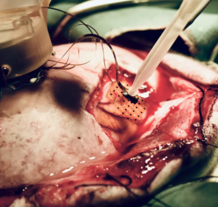
Figure 2. Design for the target: a Matrix 3D array inserted into cortex in a large-animal preparation, combined with an ECoG thin-film grid for surface and depth recording in one experiment.
What does the fabrication process decide?#
The process decides whether the probe is the design. NeuroNexus silicon probes and polymer grids are made by thin-film microfabrication, the approach that produced the first silicon microelectrodes and multisite probes at the University of Michigan (Wise et al. (1970) ↗; Najafi et al. (1985) ↗) and that NeuroNexus has refined as a proprietary production process since 2004. Four properties of a finished array are set here, and each can be measured.
Feature fidelity. A site drawn at 177 µm² is 177 µm² on every probe on the wafer, because impedance follows area; a trace drawn at a given width holds that width along its whole length, because resistance follows cross-section. NeuroNexus fine-feature lithography places sites and traces at the sub-micron scale on a shank a few tens of micrometers wide. The evidence is the impedance distribution across a probe's sites: when the sites are the size they were drawn, the impedances cluster tightly around the value the area predicts, 200 kΩ to 1 MΩ at 1 kHz for a 177 µm² iridium site, and an outlier is a defect, not noise.
Insulation integrity. Each trace runs the length of the shank under a dielectric layer, beside its neighbors, in a conductive electrolyte. A pinhole in the dielectric is a leak to the tissue, which reads as a site that is not where the design put it; a thin spot between traces is crosstalk, which reads as the same spike on two channels that should not share it. The layer stack, substrate, dielectric, traces, a second dielectric with vias opened through it, sites and bond pads, is only as good as its weakest deposition, and the failure surfaces in the recording rather than on the bench.
Uniformity and yield. A process that produces one working probe per wafer and a process that produces a wafer of working probes are different processes, and the difference is what the laboratory receives. NeuroNexus batch fabrication puts several designs on one wafer and makes every probe of a design under the same conditions, so probes are identical rather than similar. The evidence is site yield, the fraction of sites on a delivered probe that read within range, and its consistency from probe to probe and lot to lot.
Release and handling. The last step lifts individual arrays from the wafer and sends them to assembly. A shank stressed at release, or a site surface contaminated between release and packaging, is a defect the process introduced after the design was already correct. NeuroNexus therefore follows fabrication with inspection and measurement, and the impedance measured at the factory becomes part of each probe's record.
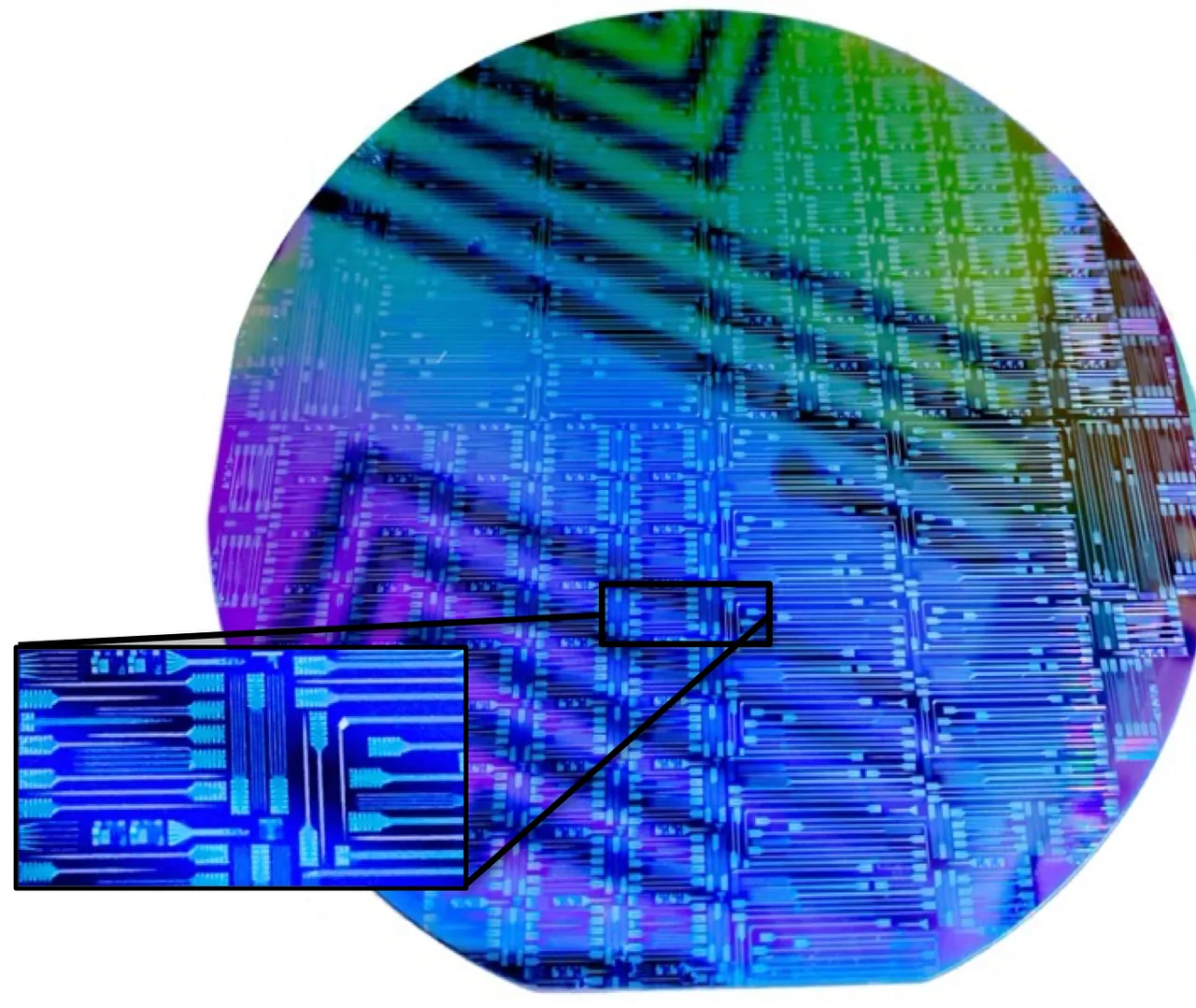
Figure 3. Batch fabrication: a wafer of NeuroNexus probes before release, with an inset of individual shanks and bond pads. Every probe of a design is made under the same conditions.
What do the materials decide?#
The materials decide how the probe behaves at the interface and how long it lasts. Four layers do four jobs, and NeuroNexus chose each material for its job; the published evidence behind each is collected in NeuroNexus Probe Technology: Questions and Answers.
The site metal is the neural interface. Iridium, on 209 of the 216 catalog silicon designs, forms a stable interface in tissue and passes charge reversibly, so it records and stimulates on the same site; SIROF (sputtered iridium oxide film), available as a site option, provides lower impedance, nominally below 100 kΩ at 177 µm², and high charge-injection capacity for stimulation (Cogan (2008) ↗). Platinum, on the thin-film grids and the SiNAPS designs, is the established choice for surface recording and active-pixel arrays. A site metal must not corrode, delaminate, or change its surface over weeks in tissue, because each of those reads as impedance drift, and impedance drift reads as a probe that is failing.
The traces route the signal. NeuroNexus uses a proprietary multilayer metal stack, optimized for feature size, adhesion, electrical resistance, and manufacturability, deposited and patterned under the same controlled process as the rest of the device; the trace metal is never exposed to tissue, so its job is signal fidelity.
The dielectrics insulate, and they decide chronic lifetime. Moisture penetrates conventional oxide and nitride insulators over weeks, which is why many thin-film electrodes that record well on the day of implantation degrade over a month. NeuroNexus uses a proprietary low-stress amorphous silicon carbide (a-SiC) as the dielectric (insulating) layer, for electrical isolation and chemical stability in tissue, including long-term chronic use. The material's performance as an implantable dielectric is well documented (Cogan et al. (2003) ↗; Deku et al. (2018) ↗).
The substrate sets the mechanics. Silicon at 15 or 50 µm is rigid enough to penetrate the brain, spinal cord, nerve, or heart, the thinner substrate displacing less tissue and the thicker one resisting buckling on long trajectories, and NeuroNexus also offers ultra-thin 5 µm designs that reduce tissue displacement and encapsulation further (Seymour and Kipke (2007) ↗); polyimide at 12 µm is flexible enough to conform to a cortical, cardiac, or nerve surface. Substrate thickness is chosen for the target and the insertion.
Coatings act on the interface. Z-Coat, the proprietary NeuroNexus PEDOT site coating, increases a site's effective surface inside the same footprint, lowering impedance by roughly an order of magnitude and raising charge capacity without changing the layout, and it is mechanically stable through repeated insertion. It is the option when a small site must record with a low noise floor or stimulate safely (Z-Coat: Optimized Site Coating for Stimulation and Noise Reduction).
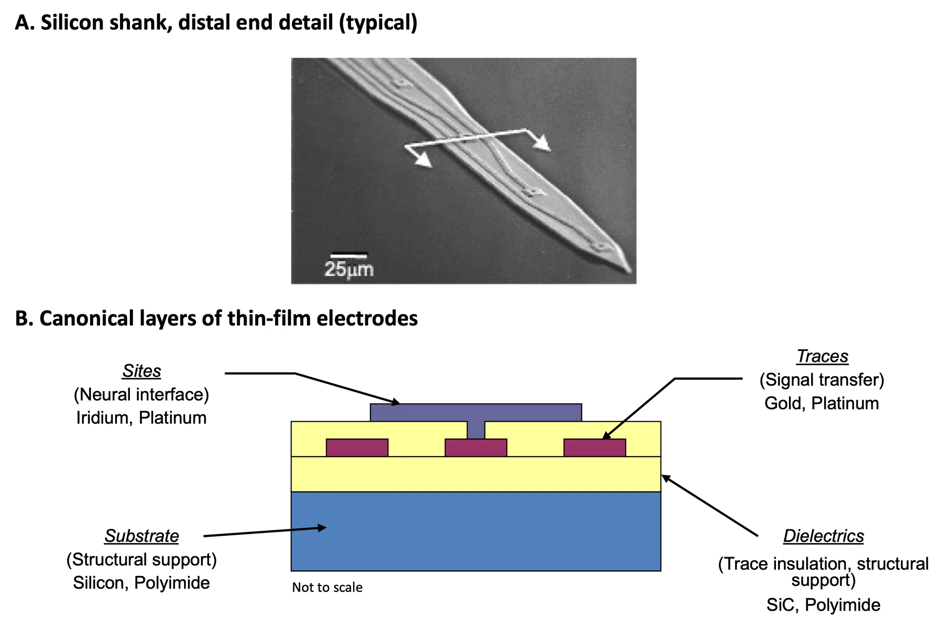
Figure 4. The materials. (A) Electron micrograph of a silicon shank tip with its electrode sites. (B) The layer stack: substrate, dielectric (insulating) layers, metal traces, and electrode sites.
What does the package decide?#
The package decides whether the array reaches the amplifier, and for how long. The connector package is the interconnect, connector, and covering assembled around the array, and it bears the mechanical load the array never sees, which is why a large share of field failures in thin-film electrodes originate there.
Three things in the package are quality determinants. The bonds from the array's pads to the interconnect must be complete on every channel and must survive handling, insertion, and, in a chronic implant, months of an animal moving against them; an open bond is a dead channel and an intermittent one is a channel that fails during the session. The insulation over the bonds and along the interconnect must be as good as the dielectric on the shank, because a leak here shorts a channel to its neighbors or to the reference just as a pinhole on the shank does. And the body must hold the array in the orientation the design assumes, under the connector's mating force and the cable's pull, without transferring that load into the silicon. NeuroNexus packages are assembled, encapsulated, and inspected by a dedicated production team, and every package series has been carried through chronic implants in published work (Vetter et al. (2004) ↗; Okun et al. (2016) ↗).
A package is also a set of decisions about use, and NeuroNexus offers fourteen package series so that the decisions fit the preparation: a rigid printed-circuit board for a stereotaxic holder in acute work; a small, light body for a chronic implant in a mouse; a flexible polyimide cable between array and connector for a floating chronic implant; a microdrive for depth adjustment; a stainless-steel support body for a long trajectory; an optical fiber, a fluidic channel, or a second array where the experiment needs one on the same trajectory; and non-magnetic parts for MRI. The same array can be ordered on several of these, so the package is a separate decision from the design, and Choosing a Probe Package treats it as one.
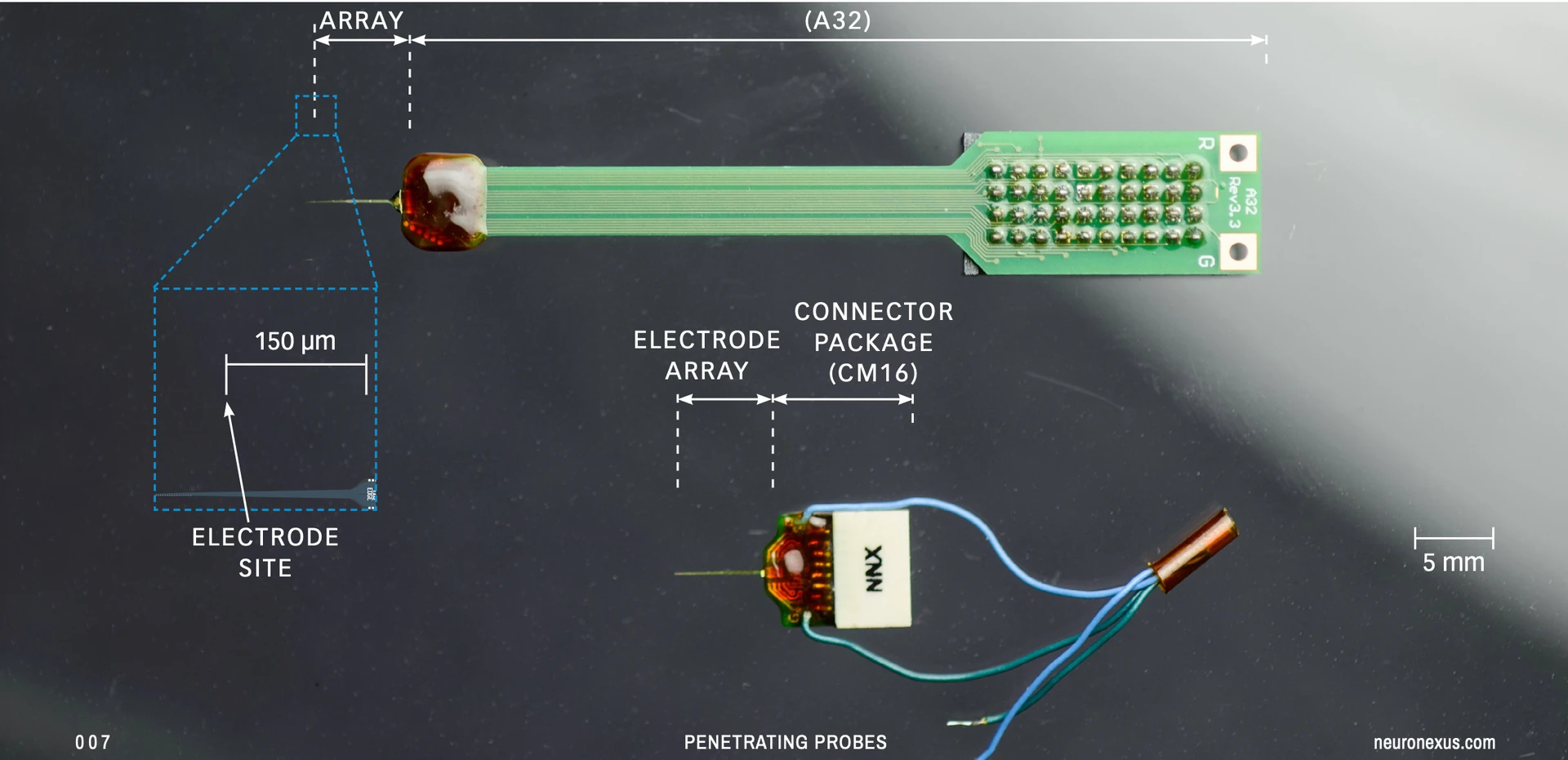
Figure 5. The package: the electrode array joined to its connector package, on an A32 package (top) and a CM16 package (bottom). Bonds, encapsulation, and body are where field failures are prevented.
How does NeuroNexus control quality?#
Quality is controlled at every stage rather than inspected in at the end. Every catalog design has a documented specification and a datasheet that records its geometry, site area, substrate, and package options, so what is ordered is what is delivered. Every probe of a design is made under the same batch conditions on the same proprietary process. After release, arrays are inspected, and after packaging, every site is impedance-tested; that factory measurement is the baseline a researcher compares against on first use and after every session, and Silicon Probes: Setup, Handling, Cleaning and Care begins with it. Site yield and impedance consistency are tracked from probe to probe and lot to lot, so a cohort receives identical electrodes. NeuroNexus controls the design, the process, and the intellectual property end to end, which is what makes lead times plannable and the catalog reproducible from one year to the next.
What support comes with the electrode?#
An electrode is chosen, inserted, cleaned, and reused, and each step is where a study is won or lost. NeuroNexus Application Scientists help match the probe geometry and package to the preparation before the order, and remain an inquiry or a phone call away afterward; the company's engineers and scientists hold more than 150 years of cumulative neural-interface design experience, and the same team runs NIH-funded research programs in-house with Harvard, Mayo Clinic, and Purdue, so the advice reflects current practice at the frontier. The documentation is written to the same standard: surgical guides for acute and chronic preparations, setup, handling, cleaning, and care procedures, a glossary of every design parameter, connectivity and compatibility guides, and a troubleshooting guide that starts from the impedance record. Custom geometries, materials, and packaging are designed with the laboratory and fabricated on the same process, with the same quality controls, as the catalog.
What does the published record show?#
NeuroNexus technology has appeared in more than 5,100 peer-reviewed publications across neuroscience and bioengineering, in more than 1,000 laboratories on six continents, over 22 years, a published record that no other thin-film probe line approaches. That record is the field's own validation, in species from fruit flies (Van De Poll and van Swinderen (2025) ↗) to non-human primates (Thirunavukkarasu et al. (2026) ↗; Perich et al. (2026) ↗), from acute recordings to chronic implants of months (Vetter et al. (2004) ↗; Okun et al. (2016) ↗; Haghighi et al. (2025) ↗), and from single-unit isolation to large-scale ensemble recording (Buzsáki (2004) ↗). It is also the record that other probe designs are measured against: when a new flexible probe is evaluated, a NeuroNexus silicon probe is the comparator (Mueller et al. (2025) ↗). These papers illustrate a small fraction of the applications; the NeuroNexus scientific publication database holds the rest.
Figure 6. The record: more than 20 years of thin-film electrodes, more than 5,000 peer-reviewed publications, more than 1,000 laboratories on six continents, and designs, processes, and software developed in-house.
How do you tell a good electrode from a poor one before it goes in?#
Measure it. Every determinant above leaves a signature that an impedance meter, a microscope, and a session log can read, and the checks take less time than a failed session costs.
Impedance, every site, before every session. The distribution across sites is the single most informative number a probe gives. A good array reads tightly: for 177 µm² iridium sites, most values between 200 kΩ and 1 MΩ at 1 kHz, with a spread that reflects the area tolerance and little else. A site far above the cluster has a broken trace, an open bond, a contaminated surface, or a dried residue; a site far below has a short to a neighbor or to the reference. A cluster that has moved upward as a whole since the last session is a surface that needs cleaning or, in a chronic implant, tissue response. The probe setup procedure begins with this measurement, and the factory record gives the baseline.
Crosstalk. Two channels that show the same spike at the same amplitude are one neuron and a leak, not two neurons. In a bench test, a signal applied to one site should not appear on another; in tissue, a unit that appears identically on non-adjacent sites is a defect, not a finding.
Visual inspection. Under a microscope, sites are clean and uniform, traces continuous, the shank free of cracks at the base and the tip, and the bonds and their insulation intact. Most of what an impedance meter reports can be seen.
Stability across sessions. A good probe reads the same impedance after cleaning as before the session, across many sessions; a probe whose sites climb session over session is losing its surface or its insulation. A log of per-site impedance over the life of a probe is the record that separates a probe problem from a preparation problem, and Noise Reduction and Troubleshooting starts from that record.
Consistency across probes. In a cohort, the same design reads the same distribution on every probe. When it does, differences between animals are biology; when it does not, they may be the electrode.
Why select NeuroNexus electrodes#
Judge an electrode by its determinants, not its specification: what was designed, how faithfully it was made, what it was made of, how it was packaged, and who stands behind it. NeuroNexus designs geometry for the target across the broadest thin-film design space in the field, fabricates it on a proprietary process refined over more than 20 years, builds it from materials chosen and documented for the neural interface, packages it for the preparation, tests every probe before it ships, and supports it with Application Scientists and documentation written by the people who make it. More than 5,000 publications are the result. Choosing the design is the subject of Choosing an Electrode for Your Experiment; the full range of designs is in The Electrode Design Space. Explore silicon probes and thin-film grids. The short form of this paper is Why NeuroNexus.
Related documents#
- Read next, in order: Silicon Probes and Thin-Film Grids: An Introduction · NeuroNexus Probe Technology: Questions and Answers · How an Electrode Records Neural Activity · Choosing an Electrode for Your Experiment · Choosing a Probe Package · Thin-Film Grids for Surface Recording · The Electrode Design Space
- Materials and care: Z-Coat: Optimized Site Coating for Stimulation and Noise Reduction · Silicon Probes: Setup, Handling, Cleaning and Care · Noise Reduction and Troubleshooting · A Brief History of Electrode Technology
- Glossary: Silicon probe · Thin-film grid · Thin-film microfabrication · Michigan probe · Silicon carbide dielectric · SIROF · Z-Coat · Site area · Impedance · Probe package
Citations#
- Wise, K. D., Angell, J. B., & Starr, A. (1970). An integrated-circuit approach to extracellular microelectrodes. IEEE Transactions on Biomedical Engineering, 17(3), 238–247. DOI: 10.1109/TBME.1970.4502738 ↗
- Najafi, K., Wise, K. D., & Mochizuki, T. (1985). A high-yield IC-compatible multichannel recording array. IEEE Transactions on Electron Devices, 32(7), 1206–1211. DOI: 10.1109/T-ED.1985.22102 ↗
- Cogan, S. F., et al. (2003). Plasma-enhanced chemical vapor deposited silicon carbide as an implantable dielectric coating. Journal of Biomedical Materials Research Part A, 67(3), 856–867. DOI: 10.1002/jbm.a.10152 ↗
- Buzsáki, G. (2004). Large-scale recording of neuronal ensembles. Nature Neuroscience, 7(5), 446–451. DOI: 10.1038/nn1233 ↗
- Vetter, R. J., et al. (2004). Chronic neural recording using silicon-substrate microelectrode arrays implanted in cerebral cortex. IEEE Transactions on Biomedical Engineering, 51(6), 896–904. DOI: 10.1109/TBME.2004.826680 ↗
- Seymour, J. P., & Kipke, D. R. (2007). Neural probe design for reduced tissue encapsulation in CNS. Biomaterials, 28(25), 3594–3607. DOI: 10.1016/j.biomaterials.2007.03.024 ↗
- Cogan, S. F. (2008). Neural stimulation and recording electrodes. Annual Review of Biomedical Engineering, 10, 275–309. DOI: 10.1146/annurev.bioeng.10.061807.160518 ↗
- Okun, M., et al. (2016). Long term recordings with immobile silicon probes in the mouse cortex. PLOS ONE, 11(3), e0151180. DOI: 10.1371/journal.pone.0151180 ↗
- Deku, F., et al. (2018). Amorphous silicon carbide ultramicroelectrode arrays for neural stimulation and recording. Journal of Neural Engineering, 15(1), 016007. DOI: 10.1088/1741-2552/aa8f8b ↗
- Van De Poll, M. N., & van Swinderen, B. (2025). Long-term multichannel recordings in Drosophila flies reveal altered predictive processing during sleep compared with wake. Journal of Experimental Biology, 228(11), jeb250165. DOI: 10.1242/jeb.250165 ↗
- Haghighi, et al. (2025). Piezo1 and Piezo2 ion channels in neuronal and astrocytic responses to MEA implants in the rat somatosensory cortex. International Journal of Molecular Sciences, 26(18), 9001. DOI: 10.3390/ijms26189001 ↗
- Mueller, N. N., et al. (2025). Mechanically-adaptive, resveratrol-eluting neural probes for improved intracortical recording performance and stability. npj Flexible Electronics, 9, 64. DOI: 10.1038/s41528-025-00440-5 ↗
- Thirunavukkarasu, P., et al. (2026). Laminar architecture of visual and auditory responses in the supplementary eye field of macaques. Cerebral Cortex, 36(6), bhag064. DOI: 10.1093/cercor/bhag064 ↗
- Perich, M. G., et al. (2026). Inferring brain-wide interactions using data-constrained recurrent neural network models. Neuron. DOI: 10.1016/j.neuron.2026.07.016 ↗