Silicon Probes and Thin-Film Grids: An Introduction
Silicon probes for penetrating targets and thin-film grids for surface targets: one microfabrication method, the design space, and how to select a device.
14 min read
Updated October 27, 2026

NeuroNexus · neuronexus.com · Resources
NeuroNexus offers two types of thin-film electrodes for neural and cardiac electrophysiology: silicon probes that penetrate the brain, spinal cord, nerves, ganglia, or heart to record and stimulate at precisely placed sites inside the tissue, and thin, flexible polymer grids that rest on the surface of the cortex, skull, heart, or a nerve and record the field beneath each site. Both are produced using proprietary photolithography and microfabrication processes, so each geometry is fixed on the wafer, designed for the target, and reproduced identically from device to device.
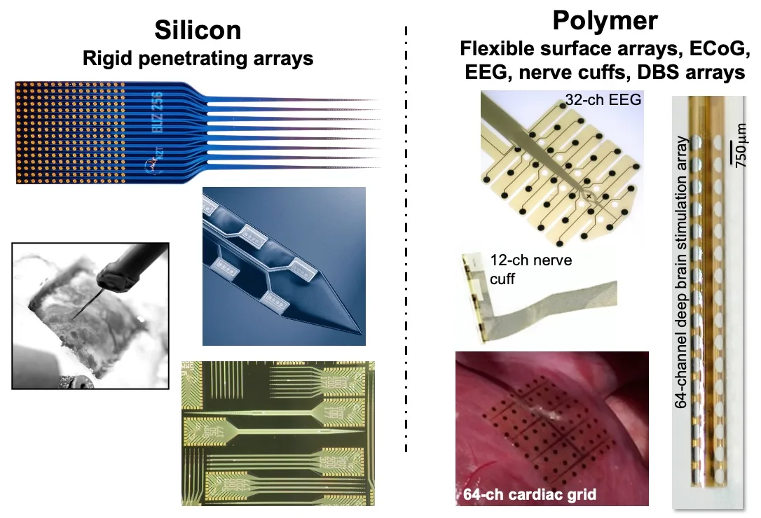
Figure 1. The two electrode platforms. (Left) Silicon — rigid penetrating arrays: a 256-site Buzsáki-layout probe die, a shank tip with its electrode sites, insertion into tissue, and dies on the wafer. (Right) Polymer — flexible surface arrays: a 32-channel EEG grid, a 12-channel nerve cuff, a 64-channel cardiac grid, and a 64-channel deep brain stimulation array.
Summary#
Electrophysiology is an important research approach because it directly measures neural or cardiac electrical activity over time and across relevant spatial scales. To do electrophysiology well, researchers need high-quality electrodes to transduce biological electrical activity, high-quality instrumentation to acquire the signals, and high-quality software to manage and analyze them. Across neuroscience and cardiac research, thin-film electrodes power both mainstream and leading-edge studies. NeuroNexus has pioneered thin-film electrodes for more than 20 years, building on the Michigan probe (Wise et al. (1970) ↗; Drake et al. (1988) ↗; Vetter et al. (2004) ↗), with a catalog of proven electrodes for diverse nervous-system and cardiac targets, plus the instrumentation and software to use them reliably.
NeuroNexus offers two general types of thin-film electrodes for different neural or cardiac targets. Silicon probes are micro-scale thin-film devices designed to penetrate the brain or heart to precisely target internal structures. Thin-film grids are thin, flexible polymer devices designed for placement on the brain, spinal cord, nerve, or heart surface. Both electrode types are made using precise photolithography and microfabrication processes to produce reproducible, reliable sensors packaged to meet experimental requirements.
This introduction makes three points.
- In electrophysiology, function follows fit: signal quality and fidelity depend directly on how well the electrode fits the target, including its geometry, materials, and placement.
- In thin-film electrode technology, the details matter. NeuroNexus has led in neural engineering for more than 20 years, and its dedicated, experienced team of engineers and scientists knows the details.
- NeuroNexus offers a catalog of thin-film electrodes, instrumentation, and software tailored to diverse anatomy, with toolchain solutions for diverse experimental protocols.
1. Function follows fit#
Nomenclature
To streamline the discussion, we will generally refer to silicon probes and thin-film polymer grids as "probes". Probes have multiple, individually addressable electrode sites (or "contacts"). Each electrode site transduces a biopotential into an electronic signal that travels along its conductive trace to the probe bond pads, then to the connector pins via the probe package. See the Getting Started Guide for additional details.
Neural interface fit, positioning electrode sites in or near the target to detect the signals of interest, begins with probe geometry, and geometry is chosen before the surgery. For a silicon probe, probe geometry is the geometry of the shanks and the spatial layout of the sites on them: shank count, length, and separation; site count, area, pitch, and layout. For a thin-film grid, it is site diameter, pitch, and array extent. Two choices are folded into that list. The first is how sites are arranged on a shank: linear spacing resolves depth and supports current source density ↗ analysis (Mitzdorf (1985) ↗); tetrode clusters give a spike sorter four views of one neuron for excellent unit isolation (Buzsáki (2004) ↗); polytrode arrangements combine isolation and coverage; and edge layouts place sites at the shank margin for minimal tissue between site and neuron. The second is how shanks are arranged in the tissue: a single shank for one target, a planar multi-shank array for lateral sampling, a three-dimensional array for a volume, and a long shank on a rigid support for a deep target in a large animal. The two choices vary independently, and NeuroNexus offers linear, tetrode, polytrode, and edge layouts on single shanks and on multi-shank arrays alike.
Materials determine what a given geometry can measure. The substrate determines how the device meets tissue: silicon at 15 or 50 µm, with ultra-thin 5 µm designs available (Seymour and Kipke (2007) ↗), is released from the wafer as a rigid shank that holds a straight trajectory into the brain, spinal cord, or heart, while 12 µm polyimide yields a flexible film that conforms to the curvature and movement of the cortex, skull, epicardium, or nerve. Site metal and site area set impedance and charge capacity. Across the probe catalog, site area ranges from 92 to 1,250 µm², and iridium is the site metal on 209 of 216 designs because it tolerates charge injection (Cogan (2008) ↗). Smaller sites isolate single units; larger sites average over more tissue and deliver more charge. When lower impedance is needed without sacrificing spatial resolution, NeuroNexus offers site coatings (Z-Coat) instead of larger sites. The materials and the published evidence for them are described in Silicon Probe Technology: Questions and Answers.
Placement completes the fit, and the package sets much of it. A design becomes an orderable probe when it is paired with a package, the interconnect, connector, and covering that fix how the device sits on the animal. Acute packages favor handling and repeated use within a session. Chronic packages favor mechanical anchoring, strain relief, and connector durability over months (Kipke et al. (2003) ↗; Okun et al. (2016) ↗); a Hybrid package uncouples the probe from the head-fixed connector via a flexible polyimide cable, and CM and X-Series packages minimize weight and profile. The package also determines the connector and cable, which determine the compatible headstage and acquisition system. Researchers typically decide acute or chronic at the start of a selection, because the package choice carries through the entire recording chain.
The six questions that turn a target into a probe name are worked through in Choosing an Electrode for Your Experiment, and the package decision in Choosing a Probe Package.
2. The details matter#
NeuroNexus makes both device classes using thin-film microfabrication, a sequence of deposition and patterning steps performed on a wafer (Najafi et al. (1985) ↗). Thin conductive and dielectric (insulating) layers (Cogan et al. (2003) ↗) are deposited sequentially on the substrate, a silicon wafer for probes or a polyimide film for grids, and each layer is patterned by photolithography using a mask that carries that layer's geometry. Every feature is transferred from the mask with the mask's precision and repeated identically on every device across the wafer, so the mask set fixes the probe geometry: shank width and length, site area, site pitch, and site layout, or, for a grid, site diameter, pitch, and array extent. The site metal, iridium on 209 of the 216 probe designs and platinum on the three active-pixel designs, is defined at the site openings, and each device is released from the wafer at its substrate thickness with one insulated conductor running from every site to a bond pad at the base. Site positions are therefore known in advance, reproducible across wafers and lots, and independent of the shank cross-section.
A finished probe has two parts. The electrode array is the microfabricated part: the shank or shanks with their sites, and a base with the bond pads where each conductor terminates. The connector package connects that base to the instrumentation through an interconnect (a rigid printed-circuit board in an A-Series package, a flexible polyimide cable in a Hybrid package, or none at all in a CM or X-Series package), a connector that a headstage mates to (Omnetics, Samtec, Hirose, Molex X3, ZIF, or CQ4), and a protective covering over the bond region. The two parts are decoupled by design: the same electrode array can be assembled into several packages, so you choose the array for the target and the package for the preparation and rig. Fourteen package series span from a four-channel Q-Trode to a 1,024-site Activus SiNAPS board, and the Activus packages integrate a digitizing headstage chip so the probe leaves the head as digital data.
Package assembly, which includes bonding, encapsulation, strain relief, and the connector, is where NeuroNexus's manufacturing experience matters most. The microfabrication process fixes the geometry, and the design fixes what that geometry measures, but the assembly determines whether every channel survives contact with the animal over months of use. NeuroNexus has designed, fabricated, and packaged thin-film electrodes for more than 20 years, and that experience is built into every catalog design and its documentation. Every catalog design records its own specification, and more than 5,000 peer-reviewed publications in more than 1,000 laboratories have used the probes. What each determinant decides, and how to check it before a probe goes in, is described in What Makes a Thin-Film Electrode Good.
3. A catalog tailored to anatomy, and the toolchain around it#
The NeuroNexus catalog is drawn against anatomy rather than channel count. It includes 216 silicon probe designs across ten families and 53 thin-film grid designs across four. Each probe family is defined by one lead attribute: A-Series sites spread along the shank for depth profiling, with polytrode and tetrode, Buzsáki, and Isomura layouts as variants; Q-Trode four sites at one depth; Matrix Array a silicon 3D probe platform; Vector Array a short array on a rigid support body for deep targets in large animals (Perich et al. (2026) ↗); HD Series an active pixel beneath every electrode, 256 to 1,024 sites (Angotzi et al. (2019) ↗); Drug Delivery a fluidic channel beside the array; and DBS Series clinical lead geometry with 32 addressable contacts. The grid families are ECoG, EEG, cardiac surface, and peripheral nerve cuff. Most shanked probe designs reach 10 mm or less, scaled to the rodent brain, and larger subjects use Vector, Matrix, and DBS designs or custom geometry; ECoG site diameters span 25 µm to 1 mm on one substrate.
NeuroNexus instrumentation and software are built to the same chain the package defines. SmartLink headstages mate directly to the package connector and digitize on an Intan RHD amplifier; X-Series headstages digitize at the head and send data over one micro-HDMI cable at any channel count. XDAQ acquisition systems record and stimulate on a single 30 kHz, 16-bit clock, and the Smartbox receives the digital stream from a SiNAPS probe with 1,024+ channels. Radiens ↗ software spans acquisition through analysis: Allego ↗ records in real time with live quality control and automatically detects hardware across Intan, Open Ephys, Plexon, and TDT systems, and Videre ↗ opens more than twenty file formats for analysis and 3D probe visualization without conversion.
The chain is configured per protocol. Fifty-four probe designs are specified for stimulation as well as recording, 103 have an optical-stimulation package option for optogenetics, 63 can be built double-sided, three integrate a microfluidic channel, and five are rDBSA leads; each is chosen at the design or package stage. When no catalog geometry matches the target, NeuroNexus designs to specification and fabricates it using the same process, so a custom design has the same reproducibility as a catalog design. Researchers can choose from established catalog configurations or work with NeuroNexus Application Scientists to design custom probes, select packages, and configure systems.
Every parameter, its catalog range, and its field in a probe name are in The Electrode Design Space; the grid families are in Thin-Film Grids for Surface Recording; the background every choice rests on is How an Electrode Records Neural Activity.
Anatomy and vocabulary#
Anatomy of a probe assembly#
A ready-to-use NeuroNexus probe assembly has two primary components: the electrode array and the connector package.
- The electrode array interfaces with neural tissue by recording brain activity or delivering stimuli through precisely placed electrode sites. NeuroNexus silicon probes are suitable for implanting into the brain, spinal cord, nerves, ganglia, and heart. Closely related thin-film grids are suitable for interfacing with the surface of these structures.
- The connector package interfaces the electrode array with external instrumentation. Each package includes a specific connector type. Researchers can pair the same electrode array with different connector packages, giving them flexibility to configure the best neural probe for their experimental requirements.
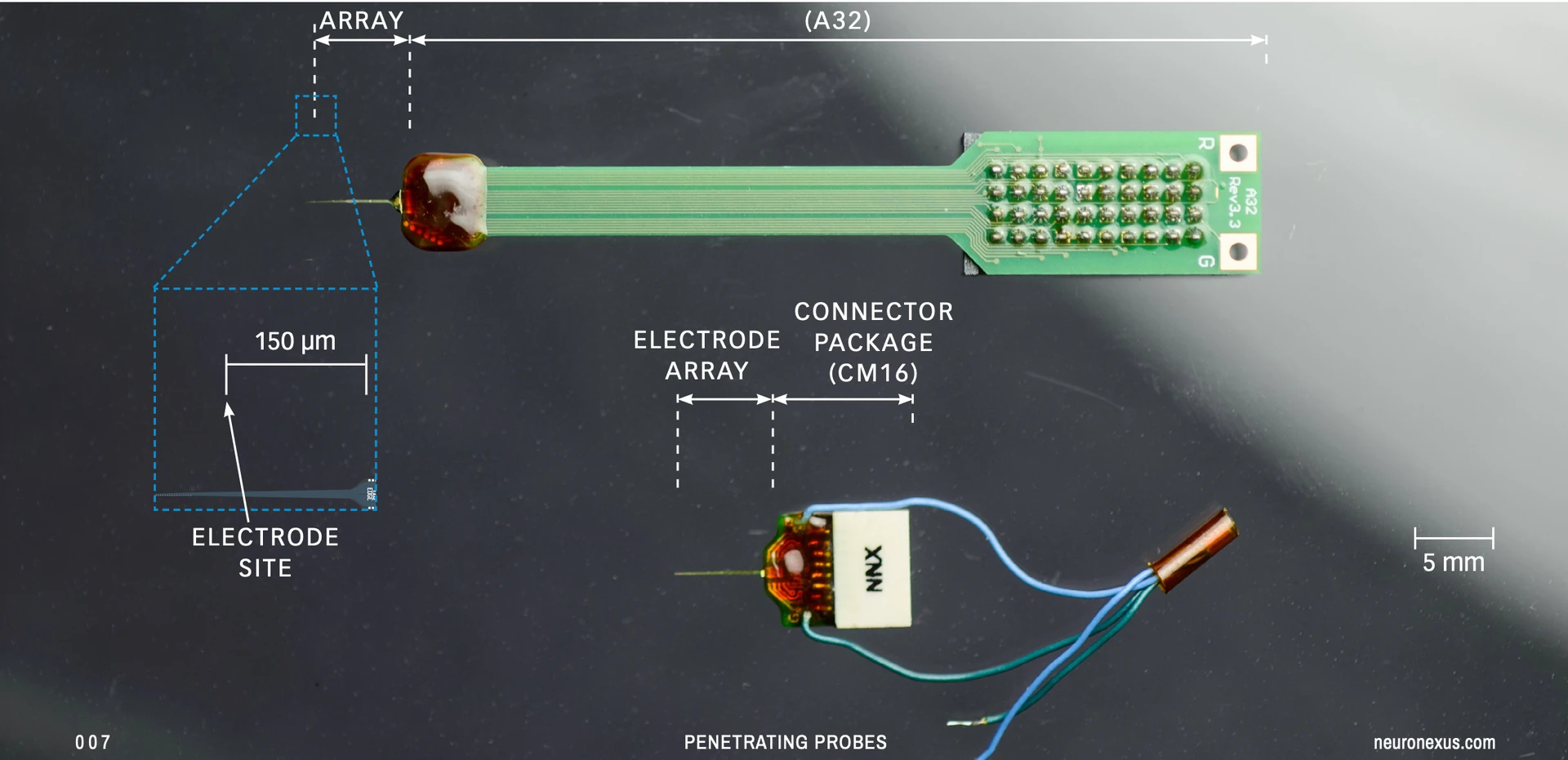
Figure 2: Canonical composition of a typical neural probe assembly. (Top) Single-shank probe mounted on A32 package. (Bottom) Single-shank probe mounted to a CM16 package, with breakout ground and reference wires.
Common probe terminology#
We generally refer to silicon probes and thin-film polymer grids as "probes". Probes have multiple, individually addressable electrode sites (or "contacts"). An electrode site transduces a biopotential into an electronic signal, which travels along its conductive trace to the probe bond pads and then to the connector pins via the probe package.
Appendix#
Thin-film microfabrication#
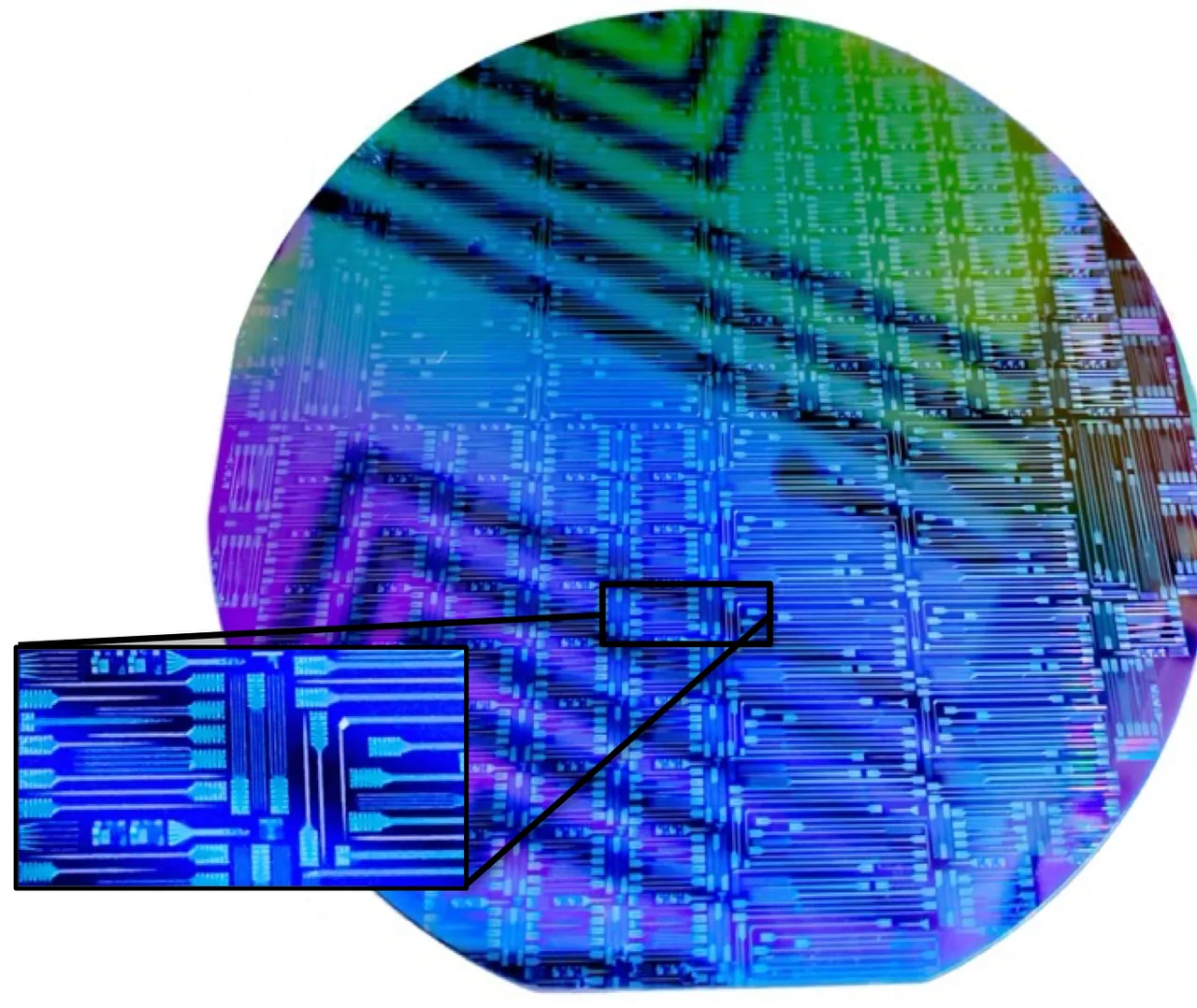
Figure 3. A silicon wafer of microfabricated probes before release, with an inset of individual shanks and bond pads.
The process is described step by step under thin-film microfabrication.
References#
- Silicon probe · Thin-film grid · Probe package · Thin-film microfabrication
- Read next, in order: How an Electrode Records Neural Activity · Silicon Probe Technology: Questions and Answers · What Makes a Thin-Film Electrode Good · Choosing an Electrode for Your Experiment · Choosing a Probe Package · Thin-Film Grids for Surface Recording · The Electrode Design Space
- Data Acquisition Systems: Overview
Citations#
- Wise, K. D., Angell, J. B., & Starr, A. (1970). An integrated-circuit approach to extracellular microelectrodes. IEEE Transactions on Biomedical Engineering, 17(3), 238–247. DOI: 10.1109/TBME.1970.4502738 ↗
- Najafi, K., Wise, K. D., & Mochizuki, T. (1985). A high-yield IC-compatible multichannel recording array. IEEE Transactions on Electron Devices, 32(7), 1206–1211. DOI: 10.1109/T-ED.1985.22102 ↗
- Mitzdorf, U. (1985). Current source-density method and application in cat cerebral cortex: investigation of evoked potentials and EEG phenomena. Physiological Reviews, 65(1), 37–100. DOI: 10.1152/physrev.1985.65.1.37 ↗
- Drake, K. L., Wise, K. D., Farraye, J., Anderson, D. J., & BeMent, S. L. (1988). Performance of planar multisite microprobes in recording extracellular single-unit intracortical activity. IEEE Transactions on Biomedical Engineering, 35(9), 719–732. DOI: 10.1109/10.7273 ↗
- Cogan, S. F., et al. (2003). Plasma-enhanced chemical vapor deposited silicon carbide as an implantable dielectric coating. Journal of Biomedical Materials Research Part A, 67(3), 856–867. DOI: 10.1002/jbm.a.10152 ↗
- Kipke, D. R., Vetter, R. J., Williams, J. C., & Hetke, J. F. (2003). Silicon-substrate intracortical microelectrode arrays for long-term recording of neuronal spike activity in cerebral cortex. IEEE Transactions on Neural Systems and Rehabilitation Engineering, 11(2), 151–155. DOI: 10.1109/TNSRE.2003.814443 ↗
- Buzsáki, G. (2004). Large-scale recording of neuronal ensembles. Nature Neuroscience, 7(5), 446–451. DOI: 10.1038/nn1233 ↗
- Vetter, R. J., et al. (2004). Chronic neural recording using silicon-substrate microelectrode arrays implanted in cerebral cortex. IEEE Transactions on Biomedical Engineering, 51(6), 896–904. DOI: 10.1109/TBME.2004.826680 ↗
- Seymour, J. P., & Kipke, D. R. (2007). Neural probe design for reduced tissue encapsulation in CNS. Biomaterials, 28(25), 3594–3607. DOI: 10.1016/j.biomaterials.2007.03.024 ↗
- Cogan, S. F. (2008). Neural stimulation and recording electrodes. Annual Review of Biomedical Engineering, 10, 275–309. DOI: 10.1146/annurev.bioeng.10.061807.160518 ↗
- Okun, M., et al. (2016). Long term recordings with immobile silicon probes in the mouse cortex. PLOS ONE, 11(3), e0151180. DOI: 10.1371/journal.pone.0151180 ↗
- Angotzi, G. N., et al. (2019). SiNAPS: An implantable active pixel sensor CMOS-probe for simultaneous large-scale neural recordings. Biosensors and Bioelectronics, 126, 355–364. DOI: 10.1016/j.bios.2018.10.032 ↗
- Perich, M. G., et al. (2026). Inferring brain-wide interactions using data-constrained recurrent neural network models. Neuron. DOI: 10.1016/j.neuron.2026.07.016 ↗